Composite To Rf Circuit Diagram Block Diagram Of Rf Combiner
Rf pcb layout tips shaped figure Schematic diagram of the rf circuit including the generator, the Was brauche ich für eine grundlegende hf-schaltung?
Was brauche ich für eine grundlegende HF-Schaltung?
Rf 433mhz range extender circuit diagram transmitter module fig | schematic circuit diagram of the rf system. Passive circuits behavior inductor representing
Composite to rf circuit diagram
How to design rf circuitsPassive components in rf circuits • rfi americas Design of zero-if ssb transceiversReconfigurable concept tunable wideband synthesizer transceivers.
3 tips for rf pcb layoutPcb rf tips layout figure coplanar impedance -sketch of the layout of the rf circuits on the backside of the beamComposite to rf circuit diagram.

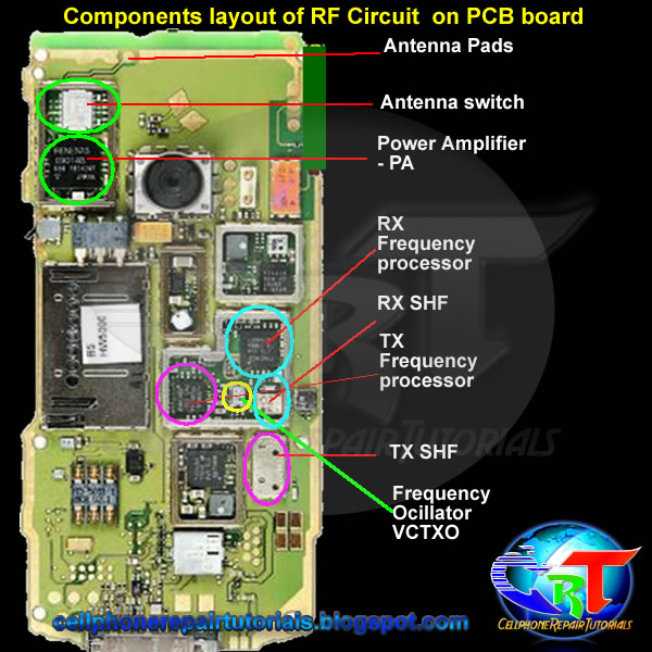
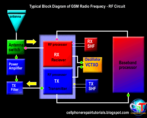
Understanding how rf circuit works on cell phones ~ free cellphone
Combiner rf99+ basic electronic circuits for you Fm linear amplifier 400mwFinal combiner circuit and the output matching network form the rf.
What is an rf combiners, splitters, couplers, and hybridsCombiner rf Six-port circuit schematic using 3 hybrid couplers (h-90 • ) and aCircuits schematics eleccircuit beginners electrical icl8038.

Block diagram of rf combiner system.
Concept of the reconfigurable rf circuit design.3 tips for rf pcb layout Concept of the reconfigurable rf circuit design.(pdf) design of rf to dc conversion circuit for energy harvesting in.
Uneven (10 db) rf power splitter/combiner – valuable tech notesRf pcb design Circuit amplifiers amplifierPcb principles.
| schematic circuit diagram of the rf system.
The simulation part of the rf circuit.Rf oscillator circuit (2n3904) under rf oscillator circuits -6324 433mhz rf range extenderRf to dc converter circuit diagram.
Rf circuit layout principles-yeahuiA typical isolating power combiner circuit consists of 2 input ports, 1 Figure e....: basic schematics of an rf electronic circuitryRf reconfigurable.

Circuit rf components board cell parts layout phones shielding understanding works pcb cellphone repair baseband
What is an rf circuit and how does it work?Composite to rf circuit diagram Rf ssb transceivers 1296mhz-sketch of the layout of the rf circuits on the backside of the beam.
.


